by Enrique Nissim, Krzysztof Okupski and Joseph Tartaro
TLDR: We present a new tool for evaluating the security of AMD-based platforms and rediscover a long-forgotten vulnerability class that allowed us to fully compromise SMM in the Acer Swift 3 laptop (see Acer's advisory).
Introduction
In the last decade, a lot of interesting research has been published around UEFI and System Management Mode (SMM) security. To provide a bit of background, SMM is the most privileged CPU mode on x86-based systems; it is sometimes referred to as ring -2 as it is more privileged than the kernel and even the hypervisor. Therefore, keeping SMM secure must be one of the main goals of the UEFI firmware.
One thing that caught our attention is that most, if not all, of the publicly available material is focused on Intel-based platforms. Since the release of CHIPSEC [1], the world has had a tool to quickly determine if the firmware does a good job protecting the system after the DXE phase and, as a result, it is hard to find misconfigured firmware in laptops from any of the major OEMs in 2022.
Make no mistake, it is not that AMD-based platforms are free from bugs [2]. Nevertheless, judging by their description, these seem to be associated with SMI handlers rather than platform security configurations. In contrast, the only presentation we found mentioning AMD platform security was done by Pete Markowsky in 2015 [3].
This blog walks through the discovery and exploitation of a security issue that was automatically identified by an in-house developed tool.
The Tool
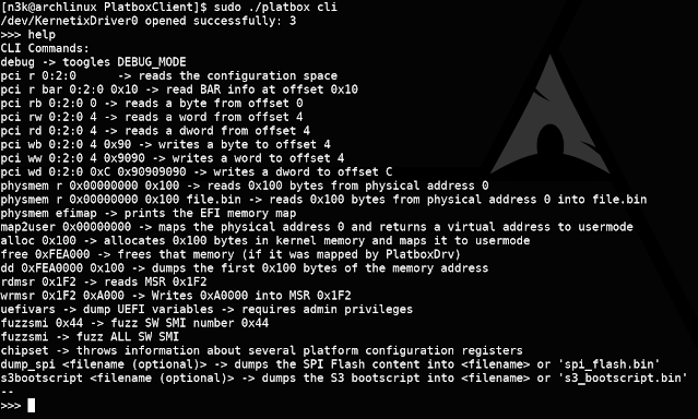
Platbox is a firmware assessment tool that allows you to retrieve chipset configuration values and interact with PCIe devices, physical memory, MSRs, and so on. The project was born back in 2018 as part of a security evaluation for an OEM's Intel-based platform; however, we recently extended it to support AMD systems.
Source code, compiled binaries, and examples can be found here: https://github.com/IOActive/Platbox
Next, we evaluate the security of one of our targets AMD systems and demonstrate how it can be used to find chipset configuration issues.
The Test-Run
In order to put our tool to the test, we ran it against the Acer Swift 3 (model no. SF314-42; BIOS v1.10), the output of which is shown below:
PS C:\Users\IOActive\Desktop\Platbox\PlatboxClient> .\build\build64\Release\platbox_cli.exe cli
>>> chipset
MemoryRange: fe000000
RomProtect_0
- Base: ff73a000
- RangeUnit: 1
- Range: 00000039
- Protected size: 00390000
- WriteProtected: 1
- ReadProtected: 0
- Total range [ff73a000, ffad9fff)
RomProtect_1
- Base: fff20000
- RangeUnit: 0
- Range: 000000df
- Protected size: 000df000
- WriteProtected: 1
- ReadProtected: 0
- Total range [fff20000, ffffffff)
RomProtect_2
- Base: 00000000
- RangeUnit: 0
- Range: 00000000
- Protected size: 00000000
- WriteProtected: 0
- ReadProtected: 0
- Total range [00000000, 00000fff)
RomProtect_3
- Base: 00000000
- RangeUnit: 0
- Range: 00000000
- Protected size: 00000000
- WriteProtected: 0
- ReadProtected: 0
- Total range [00000000, 00000fff)
SPI BASE: fec10000
SPIx1D - SpiProtectEn0: 1
SPIx1D - SpiProtectEn1: 1
SPIx1D - SpiProtectLock: 1
LPC ROM Address Range1 Start: 0
LPC ROM Address Range1 End: fffff
LPC ROM Address Range2 Start: ff000000
LPC ROM Address Range2 End: ffffffff
-> MSR:[c0010111]: 00000000AEF43000
MSR C001_0111 SMM Base Address (SMM_BASE)
=> Base: aef43000
-> SMI-Handler Entry Point: aef4b000
-> SMM Save-State Area : aef52e00
-> MSR:[c0010112]: 00000000AE000000
MSR C001_0112 SMM TSeg Base Address (SMMAddr)
=> Value: ae000000
-> MSR:[c0010113]: 0000FFFFFF006603
MSR C001_0113 SMM TSeg Mask (SMMMask)
=> Value: ff006603
-> TSegMask: ff000000
-> TMTypeDram: 6
-> AMTypeDram: 6
-> TMTypeIoWc: 0
-> AMTypeIoWc: 0
-> TClose: 0
-> AClose: 0
-> TValid: 1
-> AValid: 1
-> MSR:[c0010015]: 0000000109000010
MSR C001_0015 Hardware Configuration (HWCR)
=> Value: 9000010
-> SMMLock: 0
[...]
As we can see, the tool has extracted a variety of information from the system, namely:
- Flash protected ranges
- Flash lock configuration
- TSEG memory range
- SMM base address
- SMM lock configuration
The first part describes the protections applied to the flash that prevent any run-time access (including from SMM). Each protected range defines (i) a memory range in flash and (ii) read/write access permissions. These protections are applied at boot-time and should be locked to prevent tampering.
The second part describes protections applied to the SMM memory that prevent any run-time access from the OS. To this end, the so called TSEG region is used; the configurations include, among others, (i) the TSEG memory range and (ii) whether it is active or not. As before, these protections are applied at boot-time and should be locked to prevent modification.
Note that for the sake of brevity the remainder of the output has been truncated.
The Vulnerability
We see that the tool has found that the SMM lock configuration bit in the HWCR is set to 0. Let's try to understand why this is an issue.
According to AMD specifications [4], the SMM lock configuration bit in the HWCR is used to indicate that (i) SMM code is running in either the so called ASEG or TSEG region and (ii) that certain SMM registers are read-only:
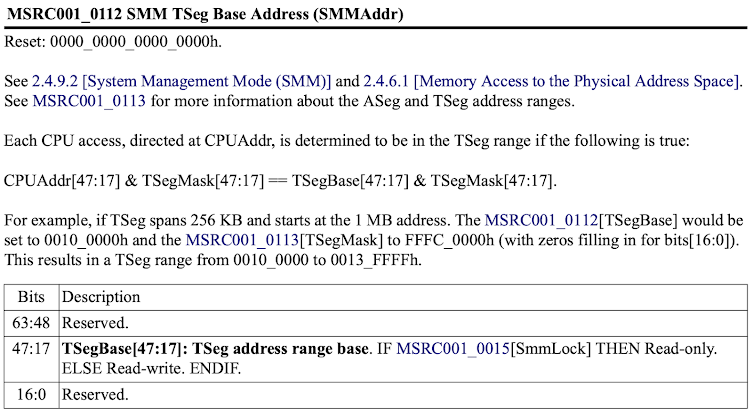
The reference to another section at the end of the definition provides further clarification: it states that specifically MSRC001_0112 and MSRC001_0113 registers are configured to be read-only when the SMM lock bit is set:
Digging deeper into the aforementioned registers, we see that the MSRC001_0112 register corresponds to the TSEG base address. This is the base address of a protected memory region that can only be accessed when the CPU is in SMM.
The MSRC001_0113 register, on the other hand, is the TSEG mask that configures, among others, the size of the protected TSEG region, the memory range type and whether the TSEG or ASEG region should be enabled.
However, the definition of this register also tells us an important fact, namely that the ASEG and TSEG region are used to securely store SMM code and data so that it cannot be accessed when the CPU is not in SMM. If we can disable these regions, we can directly access SMM memory from the kernel.
The bits controlling whether the ASEG and TSEG regions are enabled are bit 0 and bit 1 in the SMM mask register, respectively. By setting these bits to 0, the protections should be disabled.
Having found this issue in a relatively modern system came as quite a surprise, as it was first documented by Duflot et. al. in 2006 [5] and since then, at least for Intel platforms, OEMs have basically eradicated it.
Exploitation
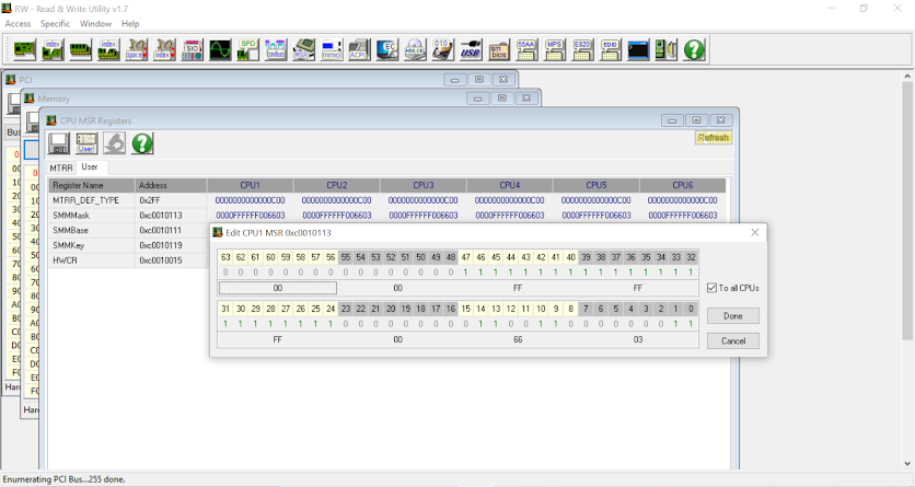
To exploit this vulnerability, we run the Read&Write Utility and add the SMM TSEG mask register to the list of custom MSR registers:
Next, we set the last two bits, corresponding to the ASEG and TSEG valid bits, on all CPUs to 0:
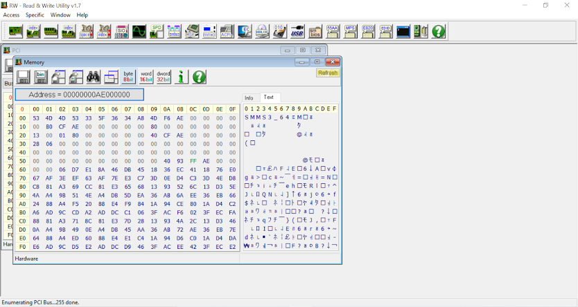
Finally, we confirm that the beginning of the TSEG region is accessible by inspecting the memory:
From here on exploitation is trivial as we have full read and write access to SMM memory.
Here is the SMRAM dump for those who want to perform additional analysis on it:
https://github.com/IOActive/uefi_research/tree/main/acer_swift_3_sf314_42
Timeline
- 06 August 2022: Reported vulnerability
- 22 September 2022: Confirmed vulnerability and working on fix
- 14 October 2022: Discussing timelines
- 18 October 2022: Confirmed patch release date
- 20 October 2022: Patch released
- 24 October 2022: Acer published bulletin
References
[3] Ring -1 vs Ring -2: Containerizing Malicious SMM Interrupt Handlers on AMD-V, Pete Markowsky
[4] BIOS and Kernel Developer's Guide (BKDG) for AMD Family 15h Models 70h-7Fh Processors, Revision 3.09, AMD
[5] Using CPU System Management Mode to Circumvent Operating System Security Functions, Duflot et al
